At ISSCC 2007, Hitachi, Ltd. and Renesas Technology Corp. have delivered a lecture (lecture number 26.6) about their micro RFID tag (wireless tag) IC measuring only 0.05 x 0.05 x 0.005 mm. This is as small as 2/27 their "next-generation mu-chip" measuring 0.15 x 0.15 x 0.0075 mm announced at the preceding ISSCC in 2006. This IC was manufactured using 90-nm CMOS technology using SOI substrates. It features a three-layer metal wiring layer and a 21 x 32 μm memory chip capable of recording 128-bit data. It is attached to a separately-provided external antenna when used, and communicates with the RFID tag reader via the 2.45 GHz band. Maximum communication range is 300 mm. Mitsuo Usami, Senior Chief Researcher at Hitachi's Central Research Laboratory who delivered the lecture, said its power when transmitting data is "slightly less than 1 mW."
Like the preceding 0.15-mm square model, this RFID tag IC also features electrodes on both surfaces for antenna connection. It is because, considering the IC's micro size, it will cost too much if manufacturers have to distinguish which side is which when they bond it to the antenna. Therefore, Hitachi and Renesas made the chip have electrodes on both sides, so manufacturers no longer need to adjust its direction and location when bonding it. It assumes to be mounted on antennas with around 6-cm length, like those used for current RFID tags. "ACF" (anisotropic conductive film) is used to bond an antenna and the IC.
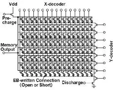
Electronic beam (EB) is used for the memory part's lithography. As the reasons to have employed EB, Usami cited (1) it allows easy manufacturing of finer transistors in the future, (2) memory chips manufactured using EB can maintain high reliability even in a high-temperature environment at 400 degrees, and (3) it requires no one-time use only mask to mark unique ID patterns. EB equipment is known to cost a lot, but Usami insisted, "This time, we can make 4 million IC chips out of a wafer sheet. This winds up concerns about EB costs. By making an IC chip much smaller, we became able to use an extravagant lithography technology rather more easily than before."
He also explained Hitachi employed SOI substrates for manufacturing process technology to enhance isolation from factors including parasitic capacity of the IC's peripheral components. "Downsized ICs tend to cause more latch-up occurrence due to parasitic capacity of other components around the IC, among other factors, and adverse voltage might run into the IC depending on circumstances. We used to add a guard ring to prevent this before, but what mattered was a guard ring resulted in a larger IC. SOI substrates were essential to the size reduction," said Usami.
Hitachi and Renesas plan to create a 12-μm square IC by miniaturizing the manufacturing technology to 65-nm rule and then to 23-nm rule. Usami said, "If using EB, we will surely be able to miniaturize memory part as well."
A hurdle to overcome lies in PC performance required to process lithography patterns, rather than the manufacturing technology itself. Usami added, "It takes a long time for a PC to process information by linking numerous patterns. This will determine the manufacturing throughput after all."


0 comments: